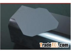


1. Wafer Diameter: (125 x 125)+/-0,4mm
2. Dimensions Tolerance: +/-0,4mm
3. Thickness of wafer, measured in the center of wafer: 190+/- 10µm, =185 µm
4. TTV: not more than 25 µm
5. Saw mark: =15 µm, invisible by eyes
6. Camber: =30 µm
7. Arc width departure(Big and small angle): =2mm in 45°
8. Surface Quality: No crack, no obvious saw mark, without obvious tactility, no pit, no V type gap, no hole, no glue left, surface cleaned, no abnormal spot, no stain.
9. Notch: not allowed
10. Tiny luminance Edge: Width =1/3 of wafer thickness; Length=1/2 of wafer dimension
11. Edge defect: Edge defect width =0.2mm; extension less than 0.5mm; with total quantity =2, distance=30mm
silicon wafer

Tangshan Guofeng Screws Co.,Ltd
